Difference between revisions of "TF EIM Chapt5"
| (41 intermediate revisions by the same user not shown) | |||
| Line 12: | Line 12: | ||
{| border="3" cellpadding="20" cellspacing="0" | {| border="3" cellpadding="20" cellspacing="0" | ||
| − | |[[File:TF_EIM_ForwardBiased_bottomhalfBipolar.jpg| 200 px]] | + | |[[File:TF_EIM_ForwardBiased_bottomhalfBipolar.jpg| 200 px]] |
|- | |- | ||
| − | | The n-p junction. The depletion region is represented as the shaded square | + | | The n-p junction. The depletion region is represented as the shaded square |
|- | |- | ||
| − | |[[File:TF_EIM_ReverseBiased_tophalfBipolar.jpg| 200 px]] | + | |[[File:TF_EIM_ReverseBiased_tophalfBipolar.jpg| 200 px]] |
|- | |- | ||
| − | | The n | + | | The p-n junction. The depletion region is represented as the shaded square. Notice the depletion region (and E-field in that region) is larger than the forward biased n-p juntion |
|- | |- | ||
| − | |[[File:TF_EIM_BipolarJunction.png| 200 px]][[File:TF_EIM_pnpBipTran.png| 200 px]] [[File:TF_EIM_BipolarJunctionDiodeRep.png| 200 px]] [[File:TF_EIM_BipolarJunctionCircuit.png| 200 px]] | + | |[[File:TF_EIM_BipolarJunction.png| 200 px]][[File:TF_EIM_pnpBipTran.png| 200 px]] [[File:TF_EIM_BipolarJunctionDiodeRep.png| 200 px]] [[File:TF_EIM_BipolarJunctionCircuit.png| 200 px]] |
|- | |- | ||
| − | | The n-p junction. | + | | The p-n-p junction. |
|- | |- | ||
|} | |} | ||
| − | The bottom p-n junction, when forward biased, provides a large current with a small voltage bias. | + | The bottom p-n-p junction, when forward biased, provides a large current with a small voltage bias. |
The top half of the p-n-p transistor is reversed biased, providing a "throttle" for the large current from the lower half. | The top half of the p-n-p transistor is reversed biased, providing a "throttle" for the large current from the lower half. | ||
| Line 37: | Line 37: | ||
:<math>\Rightarrow I_E = I_B + I_C</math> | :<math>\Rightarrow I_E = I_B + I_C</math> | ||
| − | Here it is the case that the positive current is actually representing the flow of positively charged holes (in | + | Here it is the case that the positive current is actually representing the flow of positively charged holes (in conductors the current is in the opposite direction of the flowing electrons) |
| Line 86: | Line 86: | ||
==vertical diffuse planar transistor== | ==vertical diffuse planar transistor== | ||
| − | Instead you start with a pure crystal of silicon that has been doped to to form the type | + | Instead you start with a pure crystal of silicon that has been doped to to form the type of semi-conductor you wish to have as the COLLECTOR. |
For now let's assume p-type, this means you dope pure silicon with boron. The collector is big (thick) because it has a lot of heat to dissipate. | For now let's assume p-type, this means you dope pure silicon with boron. The collector is big (thick) because it has a lot of heat to dissipate. | ||
| Line 114: | Line 114: | ||
#Molecular Beam Epitaxy: This uses a beam of particles (electrons) to heat material under vacuum such that the material evaporates and then condenses on a substrate above the crucible. Similar to Vapor-phase Epitaxy. | #Molecular Beam Epitaxy: This uses a beam of particles (electrons) to heat material under vacuum such that the material evaporates and then condenses on a substrate above the crucible. Similar to Vapor-phase Epitaxy. | ||
| − | == | + | =Bipolar Circuits= |
| + | |||
| + | == Ideal circuit== | ||
| + | |||
| + | [[File:TF_EIM_BipolarJunctionCircuit.png| 400 px]] [[File:TF_EIM_BipolarTans_DiodeEqCirc.png]] | ||
| + | |||
| + | |||
| + | The above represent an ideal circuit in which the emitter terminal is shared between the input and output voltage. This is referred to as the "common emitter" configuration. | ||
| + | |||
| + | Holes are the majority carriers in the PNP Bipolar transistor. This becomes evident if you look at how the batteries are attached. Note: the "holes" flow only in the semiconductor itself and while electrons flow in the circuit external to the semi-conductor in response to how the holes are flowing in the semi-conductor. | ||
| + | |||
| + | |||
| + | The base-emitter junction configured to be a forward biased diode and the base-collector junction is reverse biased. So the base is more "negative" than the emitter and the collector is more "negative than the base. | ||
| + | |||
| + | |||
| + | The current flow (<math>I_B</math>) is the result of electrons flowing into the base to combine with holes that are moving from the emitter to the base. Electrons exit the battery <math>V_{BE}</math> and flow to the base to combine with holes and electrons exit the emitter toward the positive battery terminal creating holes in the emitter which diffuse into the base. The recombination that takes place in the base is small compared to what takes place in the collector due to the thin base thickness and the large electric field produces by the expanded depletion region caused by the reverse biasing of the collector. | ||
| + | |||
| + | I_B -vs- V_{BE} looks like a forward biased diode. | ||
| + | |||
| + | [[File:TF_EIM_Ib-vs-Vbe_Si_Ge.jpeg | 200 px]] | ||
| + | |||
| + | The current<math> I_C</math> (and<math> I_B</math>) are produced when holes move from the emitter to the collector and meet electrons which are supplied by the battery <math>V_{CE}</math>. If you look at the relationship between <math>I_C</math> and<math> V_{CE}</math> you will see two regions. | ||
| − | + | The Active mode region represent the situation in which the p-n junction of the collector and base is reverse biased such that holes from the emitter can travel to the collector with little chance of recombining in the base. In this region, small changes in the base current result in large changes in the collector current while the potential difference between the collector and emitter is constant. | |
| − | + | The Saturation region occurs at low<math> V_{CE}</math> voltage and represents the situation just before reverse biasing turns on the flow (cut-in voltage), in essence both p-n junctions are forward biased so the collection current depends on the collector-emitter Voltage <math>V_{CE}</math>. | |
| + | [[File:TF_EIM_pnp_Charac_Ic-vs-Vce_Curve1.gif]][[File:TF_EIM_pnp_Charac_Ic-vs-Vce_Curve2.gif]] | ||
== Testing for pnp or npn== | == Testing for pnp or npn== | ||
| Line 148: | Line 170: | ||
| npn||low || high|| low||high ||high || high | | npn||low || high|| low||high ||high || high | ||
|} | |} | ||
| + | |||
| + | ==Load Line== | ||
| + | |||
| + | |||
| + | The load line represents the bias conditions in which the <math>I_C -vs V_{CE}</math> dependence is linear;(i.e.: a constance Resistance). Setting up a circuit which changes the transistor bias along the load line means that the transistor is behaving like a resistor. | ||
| + | |||
| + | |||
| + | Consider the collector-Emitter side of the transistor below. | ||
| + | |||
| + | [[File:TF_EIM_LoadLineCircuit1.gif | 500 px]] | ||
| + | |||
| + | |||
| + | Kirchoff's loops theorem is | ||
| + | |||
| + | <math>V_{CC} - I_CR_C -V_{CE} = 0</math> | ||
| + | |||
| + | <math>\Rightarrow</math> | ||
| + | |||
| + | <math>I_C = \frac{V_{CC}}{R_C} - \frac{1}{R_C} V_{CE}</math> | ||
| + | |||
| + | A graph of <math>I_C -vs- V_{CE}</math> is a line with a slope of<math> - \frac{1}{R_C}</math> and a y-intercept of <math>\frac{V_{CC}}{R_C}</math>. | ||
| + | |||
| + | If <math>I_C=0</math> then <math>V_{CE} = V_{CC}</math>. | ||
| + | |||
| + | The point Q_0 in the above curve represents a "Quiescent" (quiet) point where the best amplification occurs because it is in the middle of the operating point. If you are designing an AC amplifier you will want to be at this point to have a wide amplifier range. | ||
| + | |||
| + | If you want to use the transistor for an analog signal (microphone-speaker) then you will want to operate the circuit near Q_0 and have a shallow load line. | ||
| + | |||
| + | Q_0 is the cutoff point where there is no output:ie; the base current is zero; the transistor has infinite resistance | ||
| + | |||
| + | Q_S is the point where the amplifier is saturating. The transistor is supplying its max current a signal going beyond will essentially be clipped. The transistor has an effective resistance of zero at this point. | ||
| + | |||
| + | |||
| + | |||
| + | If you want to make a digital switch then you want the load line as steep as possible so the circuit changes from Q_0 (off) to Q_S(on) as fast as possible. | ||
| + | |||
| + | ==Temperature Dependence== | ||
| + | |||
| + | The voltage drop <math>V_{BC}</math> is a reverse voltage drop for the majority charge carriers BUT a forward voltage for the minority carriers. | ||
| + | |||
| + | As the temperature increases the impurity atoms tend to diffuse through the semiconductor from high concentration regions to low concentration regions. | ||
| + | |||
| + | |||
| + | This means that for a pnp transistor, the thermally created electrons in the n-type base semiconductor will move towards the p-type emitter by crossing the base-emitter junction due to the forward voltage. | ||
| + | |||
| + | Similarly thermally excited holes in the p-type collector will flow to the p-type emitter due to the reverse voltage drop. | ||
| + | |||
| + | ;<math>I_{CBO}</math> | ||
| + | : The reverse current from the Collector to the Base with the emitter Open | ||
| + | |||
| + | The total current becomes | ||
| + | |||
| + | :<math>I_C = \alpha I_E + I_{CBO}</math> | ||
| + | |||
| + | As<math> I_{CBO}</math> increases with temperature, the base voltage <math>V_B</math> becomes more positive (the increase <math>I_{CBO}</math> increases <math>V_{BE}</math> and thus you need less <math>V_B</math> to overcome the the base-emitter junction). | ||
| + | |||
| + | :<math>V_{BE} = V_B - V_E</math> | ||
| + | |||
| + | As <math>V_B</math> goes more positive, <math>I_C</math> and <math> I_E</math> increase, and thus the temperature of the semiconductor will increase. | ||
| + | |||
| + | The base current becomes | ||
| + | |||
| + | :<math>I_B = (1-\alpha)I_E - I_{CBO}</math> | ||
| + | |||
| + | The base current becomes less but it is usually kept constant by the power source. | ||
| + | |||
| + | You have "thermal runaway" and the transistor may burn out. | ||
| + | |||
| + | |||
| + | |||
| + | To compensate for this you add a resistor (<math>R_E</math>) between the base and emitter as shown below which holds <math>V_{EB}</math> constant. (Now <math>V_B</math> and <math>V_E</math> are both held constant) As <math>V_B</math> goes more positive due to the reverse current I_{CBO} the resistor <math>R_1</math> will make <math>V_E</math> go more positive as well. | ||
| + | |||
| + | |||
| + | [[File:TF_EIM_LoadLineTempControlledCircuit.png| 200 px]] | ||
| + | |||
| + | =Bipolar Transistor Amplifier= | ||
| + | |||
| + | A npn bipolar transistor amplifier configured with a common emitter is shown below. | ||
| + | |||
| + | [[File:TF_EIM_Lab14a.png]] | ||
| + | |||
| + | |||
| + | Let's build this circuit starting with the above load line circuit that has been stabilized for temperature. | ||
| + | |||
| + | [[File:TF_EIM_LoadLineTempControlledCircuit.png| 200 px]] | ||
| + | |||
| + | |||
| + | Let's add an input current for the base. | ||
| + | |||
| + | ==Setting I_B== | ||
| + | |||
| + | [[File:TF_EIM_TansAmp_1.png | 400 px]] | ||
| + | |||
| + | In the above circuit there is a DC bias voltage and an AC input. (The pulse generator in your lab has a DC offset you can use with the AC output sine wave). | ||
| + | |||
| + | In you lab you will want to set an<math> I_B</math> using the DC bias <math>V_{bias}</math> and a <math>V_{CC}</math> in order to put you in the middle of a load line. The AC input will move along that load line. | ||
| + | |||
| + | Applying Kirchoff's loop theorem on the left loop I would have | ||
| + | |||
| + | :<math>V_{in} -I_BR_B- V_{BE} - I_ER_E = 0</math> | ||
| + | |||
| + | I have combined the DC bias and the AC input to a total input voltage V_{in} | ||
| + | |||
| + | Since | ||
| + | :: <math>I_E = (\beta + 1) I_B</math> | ||
| + | |||
| + | :<math>V_{in} - V_{BE} = I_B \left (R_B + \left (\beta +1 \right) R_E\right )</math> | ||
| + | |||
| + | :<math>\Rightarrow I_B = \frac{V_{in} - V_{BE} }{R_B + \left (\beta +1 \right)R_E}</math> | ||
| + | |||
| + | |||
| + | If you know | ||
| + | |||
| + | :<math>V_{BE} \approx 0.6 Volts </math> | ||
| + | |||
| + | and | ||
| + | |||
| + | :<math>R_E = 220 \Omega</math> | ||
| + | |||
| + | Then you can set <math>I_B</math> using <math>R_B</math> for a given range of<math> V_{in}</math> | ||
| + | |||
| + | If you re-derive the load line equation considering the additional resistor R_E then | ||
| + | |||
| + | Kirchoff's law | ||
| + | |||
| + | :<math>V_{CC} - I_CR_C - V_{CE} - I_ER_E = 0</math> | ||
| + | |||
| + | assume <math>I_C \approx I_E</math> | ||
| + | |||
| + | :<math>I_C = \frac{V_CC}{R_C+R_B} - \frac{1}{R_C+R_B}V_CE</math> | ||
| + | |||
| + | [[File:TF_EIM_LoadLineEqFig.gif | 400 px]] | ||
| + | |||
| + | ;Note | ||
| + | |||
| + | In the actual circuit<math> R_B</math> is replaced by 2 resistors (<math>R_1</math> and <math>R_2</math>) that provide the input bias voltage by forming a voltage divider using <math>V_{CC}</math>. | ||
| + | |||
| + | :<math>\frac{1}{R_B} = \frac{1}{R_1} + \frac{1}{R_2}</math> | ||
| + | |||
| + | In other words | ||
| + | |||
| + | :<math>V_{Bias} = \frac{R_2}{R_1 + R_2} V_{CC}</math> | ||
| + | |||
| + | == Determining R_E == | ||
| + | |||
| + | [[File:TF_EIM_FindR_E_TransAmp.png | 200 px]] | ||
| + | |||
| + | Using Kirchoff's loop theorem again | ||
| + | |||
| + | :<math>V_{bias} - I_BR_B + I_{CBO}R_B - V{BE} -I_ER_E = 0</math> | ||
| + | |||
| + | :<math>I_B =(1-\alpha)I_E</math> | ||
| + | :<math>I_E = \frac{(I_C - I_{CBO})}{\alpha} = \frac{(I_C - I_{CBO})}{\frac{\beta}{\beta+1}}</math> | ||
| + | |||
| + | : <math>V_{bias} - V_{BE} = (I_B - I_{CBO}) R_B + I_E R_E</math> | ||
| + | :: <math>= (1-\alpha)I_ER_B +I_ER_E - I_{CBO} R_B</math> | ||
| + | :: <math>= (1-\frac{\beta}{\beta+1})I_E R_B +I_ER_E - I_{CBO} R_B</math> | ||
| + | :: <math>= \left (\frac{1}{\beta+1} \right )\frac{\beta+1}{\beta} (I_C - I_{CBO})R_B +I_ER_E - I_{CBO} R_B</math> | ||
| + | :: <math>=\frac{1}{\beta} (I_C - I_{CBO})R_B +\frac{\beta+1}{\beta} (I_C - I_{CBO})R_E - I_{CBO} R_B</math> | ||
| + | |||
| + | :: <math>=\left ( \frac{1}{\beta}R_B +\frac{\beta+1}{\beta} R_E \right ) I_C + \left ( -\frac{1}{\beta}R_B -\frac{\beta+1}{\beta} R_E - R_B \right )I_{CBO} </math> | ||
| + | |||
| + | :<math>\Rightarrow \left ( \frac{1}{\beta}R_B +\frac{\beta+1}{\beta} R_E \right ) I_C = \left (V_{bias} - V_{BE} \right ) + \left ( \frac{1}{\beta}R_B +\frac{\beta+1}{\beta} R_E + R_B \right )I_{CBO}</math> | ||
| + | |||
| + | or | ||
| + | |||
| + | :<math> I_C = \frac{ \frac{1}{\beta}R_B +\frac{\beta+1}{\beta} R_E + R_B }{\frac{1}{\beta}R_B +\frac{\beta+1}{\beta} R_E}I_{CBO} + \frac{V_{bias} - V_{BE}}{\frac{1}{\beta}R_B +\frac{\beta+1}{\beta} R_E} </math> | ||
| + | ::<math> =\frac{ \frac{1+\beta}{\beta}R_B +\frac{\beta+1}{\beta} R_E }{\frac{1}{\beta}R_B +\frac{\beta+1}{\beta} R_E}I_{CBO} + \frac{V_{bias} - V_{BE}}{\frac{1}{\beta}R_B +\frac{\beta+1}{\beta} R_E} </math> | ||
| + | ::<math> =\frac{ R_B +R_E }{\frac{1}{\beta+1}R_B + R_E}I_{CBO} + \frac{V_{bias} - V_{BE}}{\frac{1}{\beta}R_B +\frac{\beta+1}{\beta} R_E} </math> | ||
| + | |||
| + | |||
| + | using the chain rule to determine the functional dependence of small fluctuations in<math> \Delta I_C</math> | ||
| + | |||
| + | :<math>\Delta I_C = \frac{\partial I_C}{\partial I_{CBO}} \Delta I_{CBO} = \frac{\partial I_C}{\partial V_{BE}} \Delta V_{BE}</math> | ||
| + | ::<math> = \frac{ R_B +R_E }{\frac{1}{\beta+1}R_B + R_E} \Delta I_{CBO} - \frac{\beta}{R_B +(\beta+1) R_E}\Delta V_{BE}</math> | ||
| + | |||
| + | ;Note | ||
| + | : when temperature increases <math>\Delta I_{CBO}</math> is positive and <math>\Delta V_{BE}</math> is negative | ||
| + | |||
| + | For<math> \Delta T</math> = 10 degrees celsius <math>\Delta I_{CBO}</math> is about 2nA and <math>\Delta V_{BE}</math> is about -25 mV. | ||
| + | |||
| + | For most circuits <math>R_B</math> is about 10 times<math> R_E</math> | ||
| + | |||
| + | so | ||
| + | |||
| + | :<math>\Delta I_C \approx \left ( 1 + \frac{R_B}{R_E} \right) \Delta I_{CBO} - \frac{\Delta V_{BE}}{R_E}</math> | ||
| + | |||
| + | The larger <math>R_E</math> is the better the temperature stability | ||
| + | |||
| + | If <math>R_E = 500 \Omega</math> then <math>\Delta I_C \approx 0.05</math> mA | ||
| + | |||
| + | == General Observations== | ||
| + | |||
| + | 1.) Notice the input goes through a high pass filter with a break point of<math> \frac{1}{R_1 C_1}</math>. | ||
| + | |||
| + | 2.) The output also goes through a high pass filter with a break point of<math> \frac{1}{R_l C_2}</math>. | ||
| + | |||
| + | 3.) Kirchoff voltage rule | ||
| + | |||
| + | :<math>V_{CC} -I_C R_C - V_{CE} - I_E R_E = 0</math> | ||
| + | :<math>V_{CC} - V_{CE} -I_C (R_C + R_E) = 0</math> <math>I_C \approx I_E</math> | ||
| + | |||
| + | :<math>\Rightarrow I_C =\frac{ V_{CC} - V_{CE}}{R_C + R_E }</math> | ||
| + | |||
| + | 4.) Kirchoff law | ||
| + | |||
| + | :<math>V_{CC} -(I_B + I_D) R_2 - V_{EB} - I_E R_E = 0</math> | ||
| + | |||
| + | 5.) INput resistance | ||
| + | |||
| + | <math>\frac{1}{R_{in}} = \frac{1}{X_B} + \frac{1}{R_1} + \frac{1}{R_2}</math> | ||
| + | |||
| + | 6.) | ||
| + | |||
| + | :<math>V_B = \frac{R_1}{R_1+R_2} V_{CC}</math> | ||
[[Forest_Electronic_Instrumentation_and_Measurement]] | [[Forest_Electronic_Instrumentation_and_Measurement]] | ||
Latest revision as of 16:41, 2 April 2015
Bipolar Transistor
The Bipolar transistor concept
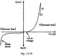
From the last chapter we saw a p-n junction diode which had similar characteristic current-vs- voltage responses when biased either in the forward direction or backward.
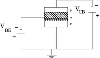
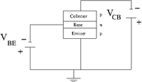
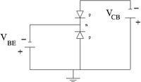
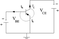
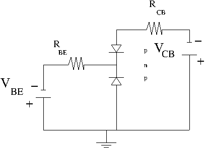
The bottom p-n-p junction, when forward biased, provides a large current with a small voltage bias.
The top half of the p-n-p transistor is reversed biased, providing a "throttle" for the large current from the lower half.
The electric field points to the "collector" in the depletion region enlarged by the reverse bias. This moves the majority charge carriers away from the collector-base junction. Once outside the depletion zone, the charge carriers rely on diffusion to escape the material.
Bipolar transistor currents
- Conservation of Current
Here it is the case that the positive current is actually representing the flow of positively charged holes (in conductors the current is in the opposite direction of the flowing electrons)
You might think that the base current is larger than the collector current because of the reverse bias on the collector which leads to the base having lower resistance than the collector.
The above is not the case.
The potential continuously draws electrons out of the emitter thus creating holes in the emitter. These holes diffuse into the base and are in a free-field region until they reach the depletion region between the collector and base.
While in the free-field region of the base they can do one of three things
- diffuse to the depletion region where they see the electric field and get swept into the collector.
- recombine with the mobile electrons in the base (the base is n-type material so electrons are the majority charge carriers)
- re-combine with electrons injected by into the base through the resistor
Usually the last two processes are more likely.
BUT if you make the emitter thin enough (less than the mean free path of the holes) then you can have the first process dominate such that most of the holes get swept into the collector before they get a chance to recombine.
As a result a large fraction of the current into the emitter () goes into the collector. ()
returning to conservation of current
So small changes in produce large changes in (You can control a large current using a small current )
- This is an amplifier!
- If you inject a signal into the base then the small changes in the base current will result in large changes in the collector current.
Making a Transistor
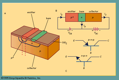
As described above, the p-n-p junction is formed by "sandwiching" a thin n-type semicondor with 2 p-type semi-conductors.
The term "sandwiching" is in quotes because you DON'T glue 3 semiconductors together.
vertical diffuse planar transistor
Instead you start with a pure crystal of silicon that has been doped to to form the type of semi-conductor you wish to have as the COLLECTOR.
For now let's assume p-type, this means you dope pure silicon with boron. The collector is big (thick) because it has a lot of heat to dissipate.
Then you dope the crystal with impurities (Phosphorus) such that a thin n-type layer is formed, by diffusion, in the middle of the p-type crystal.
You then need to treat the top layer with dopant again to overcoming the n-type characteristics which are left over from forming the n-type base in the middle of the device AND create more holes with larger dopant than the collector. This step will directly influence the gain( and ) of the transistor. The "+" label in the image below indicates that it is more p-type than the collector.
The critical feature of the process is to establish abrupt changes in the doping which create sharp boundaries.
You then coat the collector side with a conductor like metallic aluminum.
On the side used to transport dopant you need to construct contacts for the base and emitter. To do this you need an insulation layer and a conductor layer which passes through the insulation and makes contact with the base and emitter material. You use a stencil to deposit an insulating layer of SiO2 which will have holes that leave the base and emitter semiconductor material exposed. Then you deposit metallic aluminum conductor into the holes.
Epitaxial growth
The epitaxial method to create transistors is a layer-by-layer construction method in which the crystal is actually "grown" by depositing layers onto a subtrate.
There are three general methods of growing a crystal.
- Vapor-phase Epitaxy: Most common way to grow silicon. A gas like silicon tetrachloride is mixed with hydrogen. The final state of the reaction has a pure silicon silicon wafer forming and a hydrogen chloride byproduct. If the hydrogen chloride is to dense you can get some etching. The growth rate ( 2 microns/min) is known and controllable, in some cases reversible. Dopants are added to the gas for the desired semiconductor type.
- Liquid phase Epitaxy: the semiconductor ( pure or a mixture of two) is melted and grown onto a substrate by cooling at a rate of 0.1 to 1 micron/minute. Dopants are mixed into the liquid state semiconductor. Used mostly for making compound semiconductors.
- Solid Phase Epitaxy: A substrate is deposited with material. The crystal is formed by heating the solid then ions are implanted onto the crystal. The method is mostly for healing crystal damage.
- Molecular Beam Epitaxy: This uses a beam of particles (electrons) to heat material under vacuum such that the material evaporates and then condenses on a substrate above the crucible. Similar to Vapor-phase Epitaxy.
Bipolar Circuits
Ideal circuit
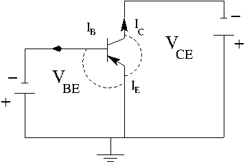
The above represent an ideal circuit in which the emitter terminal is shared between the input and output voltage. This is referred to as the "common emitter" configuration.
Holes are the majority carriers in the PNP Bipolar transistor. This becomes evident if you look at how the batteries are attached. Note: the "holes" flow only in the semiconductor itself and while electrons flow in the circuit external to the semi-conductor in response to how the holes are flowing in the semi-conductor.
The base-emitter junction configured to be a forward biased diode and the base-collector junction is reverse biased. So the base is more "negative" than the emitter and the collector is more "negative than the base.
The current flow () is the result of electrons flowing into the base to combine with holes that are moving from the emitter to the base. Electrons exit the battery and flow to the base to combine with holes and electrons exit the emitter toward the positive battery terminal creating holes in the emitter which diffuse into the base. The recombination that takes place in the base is small compared to what takes place in the collector due to the thin base thickness and the large electric field produces by the expanded depletion region caused by the reverse biasing of the collector.
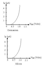
I_B -vs- V_{BE} looks like a forward biased diode.
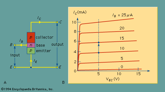
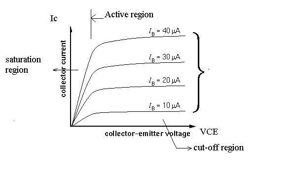
The current (and) are produced when holes move from the emitter to the collector and meet electrons which are supplied by the battery . If you look at the relationship between and you will see two regions.
The Active mode region represent the situation in which the p-n junction of the collector and base is reverse biased such that holes from the emitter can travel to the collector with little chance of recombining in the base. In this region, small changes in the base current result in large changes in the collector current while the potential difference between the collector and emitter is constant.
The Saturation region occurs at low voltage and represents the situation just before reverse biasing turns on the flow (cut-in voltage), in essence both p-n junctions are forward biased so the collection current depends on the collector-emitter Voltage .
Testing for pnp or npn
You can use an Ohmmeter to tell if a transistor is pnp or npn.
Generally the base is the middle of the three pins for a bi-polar transistor.
If you put the voltmeters positive probe on the emitter lead and the ground probe onto the base lead, then a pnp transistor will yield a low resistance (1- 10 s).
If it is a npn transistor then the positive probe on the base and the ground on the emitter will yield the small resistance.
So it you know which leads are emitter and base you can determine transistor type.
If you know transistor type, you can determine which lead is the emitter.
You can test if the transistor is good or not using the table below with the Ohmeter set on the 1 range.
| type | ||||||
| pnp | high | low | high | low | high | high |
| npn | low | high | low | high | high | high |
Load Line
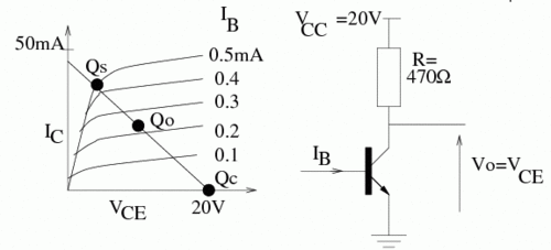
The load line represents the bias conditions in which the dependence is linear;(i.e.: a constance Resistance). Setting up a circuit which changes the transistor bias along the load line means that the transistor is behaving like a resistor.
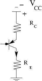
Consider the collector-Emitter side of the transistor below.
Kirchoff's loops theorem is
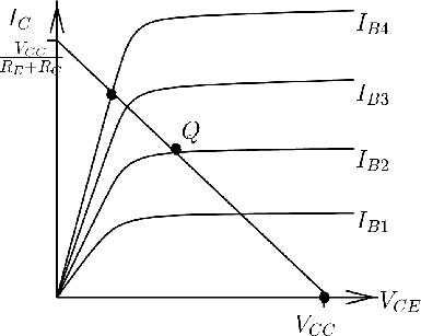
A graph of is a line with a slope of and a y-intercept of .
If then .
The point Q_0 in the above curve represents a "Quiescent" (quiet) point where the best amplification occurs because it is in the middle of the operating point. If you are designing an AC amplifier you will want to be at this point to have a wide amplifier range.
If you want to use the transistor for an analog signal (microphone-speaker) then you will want to operate the circuit near Q_0 and have a shallow load line.
Q_0 is the cutoff point where there is no output:ie; the base current is zero; the transistor has infinite resistance
Q_S is the point where the amplifier is saturating. The transistor is supplying its max current a signal going beyond will essentially be clipped. The transistor has an effective resistance of zero at this point.
If you want to make a digital switch then you want the load line as steep as possible so the circuit changes from Q_0 (off) to Q_S(on) as fast as possible.
Temperature Dependence
The voltage drop is a reverse voltage drop for the majority charge carriers BUT a forward voltage for the minority carriers.
As the temperature increases the impurity atoms tend to diffuse through the semiconductor from high concentration regions to low concentration regions.
This means that for a pnp transistor, the thermally created electrons in the n-type base semiconductor will move towards the p-type emitter by crossing the base-emitter junction due to the forward voltage.
Similarly thermally excited holes in the p-type collector will flow to the p-type emitter due to the reverse voltage drop.
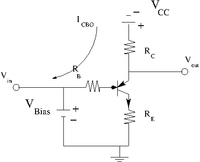
- The reverse current from the Collector to the Base with the emitter Open
The total current becomes
As increases with temperature, the base voltage becomes more positive (the increase increases and thus you need less to overcome the the base-emitter junction).
As goes more positive, and increase, and thus the temperature of the semiconductor will increase.
The base current becomes
The base current becomes less but it is usually kept constant by the power source.
You have "thermal runaway" and the transistor may burn out.
To compensate for this you add a resistor () between the base and emitter as shown below which holds constant. (Now and are both held constant) As goes more positive due to the reverse current I_{CBO} the resistor will make go more positive as well.
Bipolar Transistor Amplifier
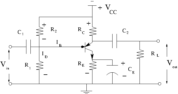
A npn bipolar transistor amplifier configured with a common emitter is shown below.
Let's build this circuit starting with the above load line circuit that has been stabilized for temperature.
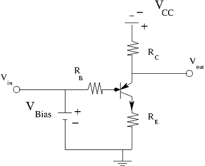
Let's add an input current for the base.
Setting I_B
In the above circuit there is a DC bias voltage and an AC input. (The pulse generator in your lab has a DC offset you can use with the AC output sine wave).
In you lab you will want to set an using the DC bias and a in order to put you in the middle of a load line. The AC input will move along that load line.
Applying Kirchoff's loop theorem on the left loop I would have
I have combined the DC bias and the AC input to a total input voltage V_{in}
Since
If you know
and
Then you can set using for a given range of
If you re-derive the load line equation considering the additional resistor R_E then
Kirchoff's law
assume
- Note
In the actual circuit is replaced by 2 resistors ( and ) that provide the input bias voltage by forming a voltage divider using .
In other words
Determining R_E
Using Kirchoff's loop theorem again
or
using the chain rule to determine the functional dependence of small fluctuations in
- Note
- when temperature increases is positive and is negative
For = 10 degrees celsius is about 2nA and is about -25 mV.
For most circuits is about 10 times
so
The larger is the better the temperature stability
If then mA
General Observations
1.) Notice the input goes through a high pass filter with a break point of.
2.) The output also goes through a high pass filter with a break point of.
3.) Kirchoff voltage rule
4.) Kirchoff law
5.) INput resistance
6.)
